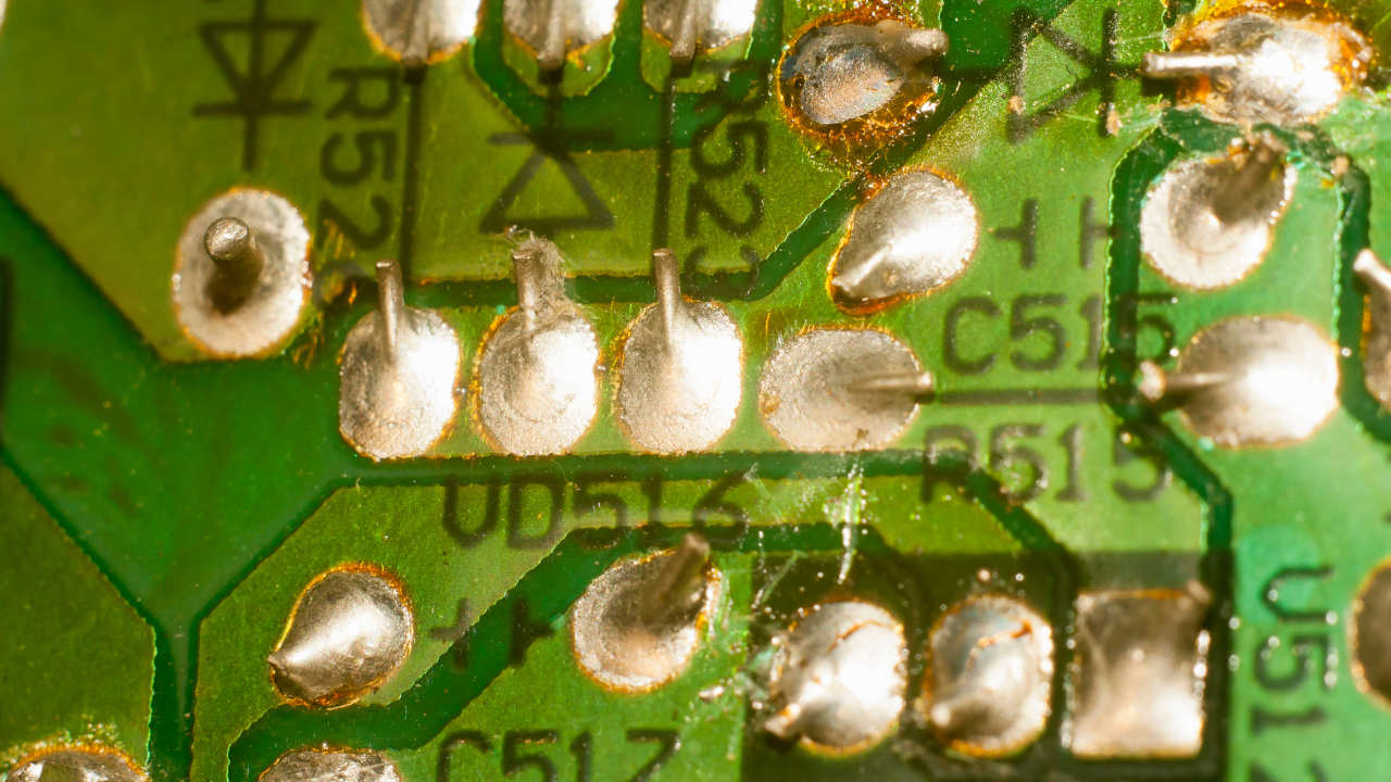
PCBs power devices like smartphones and medical equipment. At their core, PCB welding is the critical process in SMT that provides reliable electrical connections and proper component integration. Even with advanced technology, welding defects remain a major challenge.
PCB welding defects such as solder bridging, poor wetting, and so on may compromise functionality and reliability. Addressing these issues is the key to maintaining electronic devices’ performance and longevity.
Understanding Solder Bridging
Excess solder can form unintended connections between adjacent pads or components, a defect known as solder bridging. This defect is typically caused by insufficient spacing between elements, too much solder volume for the reflow process, or improper solder paste deposition. A bridge can cause a short circuit, making the device non-functional.
Precise solder paste application and correct component spacing are critical to prevent solder bridging. Optimizing reflow oven profiles is also crucial to control the solder flow. While solder bridging can occur, manual removal of the solder or the use of specialized equipment is usually enough to remove unwanted connections.
Solder Balling: A Challenge
Solder balling is a defect where the solder balls form on the PCB or component leads, causing the joint to be compromised. This is most commonly caused by excessive heat, surface contamination, or insufficient flux activity. That means these can lead to electrical shorts or weak connections.
It is just as important to keep a clean PCB surface to prevent contamination as to avoid solder balling, reflow oven temperature profiles, and flux application. In severe cases, specialized tools may need to be used to remove solder balls and reestablish the PCB’s functionality.
Cold solder joints and their implications
Cold solder joints arise when solder does not form a solid connection with the component leads or the PCB pads and, therefore, has poor electrical integrity. This defect can result in circuit failure, reduced reliability or even the complete failure of the entire device.
Cold solder joints can be detected by the naked eye, by using a multimeter, or even by using X-ray technology. Such joints require manual repair with a soldering iron or other controlled reflow methods. Reducing the likelihood of this defect involves achieving the right reflow temperature and appropriate solder deposition.
Tombstoning: A Unique Defect
Tombstoning is a soldering defect characterized by one end of a surface-mounted component on a PCB becoming elevated and resembling a tombstone. This is due to differences in preheat, solder paste deposition, and/or component leads being different sizes. It can interfere with the electrical contacts and decrease the device’s efficiency.
Thus, the issue of tombstoning can be avoided by having optimized reflow oven profiles, tight control, and quality solder paste deposition. This can be prevented through design changes, installing hold-down devices, or using adhesives in the affected areas. Appropriate attention during the manufacturing process is critical to guarantee they are well fixed on the PCB.
Solving Solder skips or inadequate solder problems involves the following steps:
Solder skips occur when the solder does not wet or make direct contact with the leads or pads, leaving gaps and creating open circuits. Inadequate soldering is characterized by a low level of solder volume, which tends to produce poor joint quality. Either of these could weaken the device’s mechanical properties and reduce its functionality and durability.
It is noteworthy that information about signals and methods of troubleshooting these types of issues includes reworking the reflow profiles and fine-tuning the solder paste deposition. Local rework options like manual adjustments or selective reflowing would be adequate in tackling these flaws. If inspection is conducted appropriately during assembly, there tends to be a reduction in skips as well as insufficient solder.
Poor Wetting: A Common Yet Critical Issue
Cold soldering occurs when molten solder is not spread and connected properly on the component leads or PCB pads. This flaw results from contamination, raw part surface conditions, or decreased flux performance.
Enhancing wetting performance begins with cleaning the PCB surfaces. Proper use of the flux and improving the surface finishes are also important tasks. Occasionally, additional processing steps or higher-value flux materials may be required for enhanced solder wetting and bonding.
Conclusion
Some of the common defects that affect the performance and reliability of the electronic device include solder bridging, solder balling, cold solder joints, tombstoning, and poor wetting. Consequently, every flaw has different roots, which one needs to address using the proper intervention approaches. It is crucial to tackle these issues to achieve high-quality PCBs that conform to the market’s requirements.
Strict inspection, changes in production processes, and quality control measures can all reduce welding defects. Thus, by using best practices, manufacturers can overcome these challenges and guarantee that communicational electronic devices will work efficiently and durably.